The receivers used in sonar are generally of the
conventional superheterodyne type with a few
added circuits that are peculiar to sonar.
The receiving systems used with the scanning
type of echo-ranging equipments are of the dual-channel type, which is required in present methods
of video portrayal. Deviation indicators, which
are cathode-ray tubes or galvanometers, use either
a sum-and-difference or a comparison receiving
system. These systems are used to measure the
phase angle of the echo signal between the two
halves of a transducer that has been electrically
split so that, on reception, it acts as two independent hydrophones. When the proper circuits
are used with these systems the phase angle can
be translated into voltage differences, and the
video portrayal is indicative of the deviation from
the correct target bearing, that isodepression deviation indication (DDI) or bearing deviation
indication (BDI). Scanning systems use conventional superheterodyne receivers-one for the
video channel and one for the audio channel. The
only function of the receiver in the video portrayal
is to furnish brightening voltage to the grid of the
cathode-ray tube because the scanning and deflection voltages are developed outside the receiver
circuits. The audio channels are used to supply
the returning echoes to the operator as an aid in
identifying targets.
The transducer used with scanning systems is
keg-shaped and is mechanically and electrically
divided into an even number of independent elements. In the model QHB-1 there are 48 such
elements located so that each element covers an
arc of 7 ½° of the transducer's periphery. On
transmission, the keying relay connects all the elements in parallel so that sound power is radiated
in all directions simultaneously, whereas on reception the elements are connected so as to form a
sharp beam in the horizontal plane. The output
of each element is connected through its individual
preamplifier to its corresponding element on each
of the two scanning switches.
The video scanning switch is driven at a constant rate and has a control transformer geared at
a 1-to-1 ratio with it. The output of this transformer controls the positioning of the electron
beam of the cathode-ray indicator so that the
electron beam synchronizes in azimuth bearing
with the scanning switch.
The audio scanning switch and the video switch
are mechanically and electrically identical, but
they differ in application. The audio switch is
positioned by a servo system and must be manually trained to the desired bearing.
These scanning circuits are called the directional
sensitivity circuits. They were discussed in chapter 6.
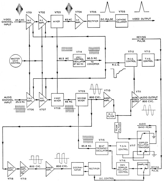
Conventional Superheterodyne Sonar Receiving System
The receiving system described in the following
paragraphs is that of the QHB-1 scanning sonar
equipment. The QHB-1 system was chosen for
discussion because its method of video portrayal
follows the conventional design and it can be considered a typical system. The block diagram is
shown in figure 7-1.
The receiver-converter includes separate video-channel and audio-channel receivers for the signals from the corresponding scanning switches.
In this system a tunable oscillator supplies a frequency to the first mixers in both channels and
also to the converter, which produces the transmitted frequency. This oscillator identifies the
149
Figure 7-1. -Block diagram of QHB-1 dual-channel receiver unit.
circuit as the unicontrol system because it enables
a single control to tune the receivers and the transmitter at the same frequency. In the receiver-converter a master fixed-frequency 65 kc oscillator
(not shown in figure 7-1) modulates a 90.5 kc
signal (arbitrarily selected) from the unicontrol
oscillator, and the 25.5 kc frequency difference is
amplified in the transmitter power amplifier.
The i-f stages of both receiver channels are tuned
to 65 kc. The first mixer in the receiver channels
150
automatically produces an intermediate frequency
of 65 kc because the 25.5 kc received signals are
mixed with the 90.5 kc output of the unicontrol
oscillator.
The frequency of the unicontrol oscillator may be
varied from 87 to 94 kc to produce a variation in
transmitted frequency of from 22 to 29 kc. The
transducer is operable between 24 and 27 kc, Although its most efficient operating point is at its
own resonant frequency-in this case, 25.5 kc.
The operation of the unicontrol oscillator will be
studied with the receiver circuits; the details of the
master oscillator will be studied in the chapter on
transmitter circuits.
A bias for the reverberation control of gain
(RCG) derived from the audio output is supplied to
the two r-f stages of the audio channel and to the
two r-f stages of the video channel. In addition,
the master gain control on the front panel of the
sonar indicator operates upon the two r-f stages of
each channel.
In the audio-channel receiver a beat-frequency
oscillator is controlled, except in the listen condition, by two types of doppler-nullifier circuits-own-doppler nullifier (ODN) and target-doppler
nullifier (TDN). The ODN circuit is operated by
ship's own doppler and restores the reverberations
to 800 cycles per second; the TDN is operated by
target echo signals and has such short response
time that it restores the audio note on target echoes
to 800 cycles per second. The doppler-nullifier
circuits are necessitated by the sharply tuned audio
circuit in this receiver. The TDN circuit can be
disabled and is used only when the audio system is
operated in the peak filter position for improvement of the signal-to-noise ratio.
VIDEO CHANNEL
The video channel of the receiving system (figure
7-2) consists of a tuned r-f stage, V701; and untuned r-f stage, V702; a mixer, V703; an i-f
amplifier, V704; and an output rectifier and cathode follower, V705.
The balanced input signal is supplied from the
video channel of the directional-sensitivity circuits
to the input transformer of the tuned r-f stage.
From this transformer it is coupled through a
suppressor resistor to the t-r-f amplifier tube.
The RCG bias for the grid circuit, derived as explained later in this chapter, is supplied to the
control grid of this stage. The cathode bias is
controlled by the master gain control on the front
panel of the sonar indicator control. The plate
load of the stage consists of an inductor and three
capacitors in parallel. One of these capacitors is a
section of the master tuning capacitor. The other
two ensure correct tracking of the circuit with the
audio t-r-f stage and unicontrol oscillator.
The voltage output across this tuned impedance
is capacitively coupled to the grid of the untuned
r-f stage. RCG grid bias is applied also to this
stage, as is the cathode bias from the master gain
control. This r-f stage uses degenerative feedback
provided by an unbypassed cathode resistor.
The output of this stage is capacitively coupled
to the control grid of the mixer. This stage operates at almost zero d-c grid bias, and uses a conventional cathode resistor for inverse feedback.
The screen voltage is produced by the cathode-follower section of the unicontrol oscillator, and
consists of a d-c component and an a-c component at the unicontrol oscillator frequency.
The i-f stage is conventional except that L-C
coupling is used rather than the standard i-f
transformer coupling. The plate and grid inductors are tuned to parallel resonance at the 65-kc
intermediate frequency. R714 serves as a parasitic suppressor.
Inverse feedback is obtained in the i-f stage
across the cathode resistor. This stage has well-decoupled plate voltage and is followed by a band
pass i-f coupling, similar to the preceding one.
The coupling capacitor, in conjunction with the
tuned i-f transformers, serves to form a band-pass
filter.
The output of the i-f stage is rectified by one-half of the twin triode, V705, connected as a
diode, and the output of this rectifier appears
across a resistive load with the i-f frequency component filtered out. This output is produced in
series with a fixed negative bias of 10 volts which
is also impressed upon the grid of the cathode-follower section of V705. The rectified signal is
coupled to this grid through an RC circuit with a
time constant of 22 milliseconds, which is adequate for pulse reception yet sufficiently short for
removing any steady-signal (low-frequency) components. The capacitor of this RC circuit must,
of course, be shorted whenever test measurements
of steady-signal levels are to be made in the
151
video-channel output. The cathode-follower section of V705 produces its output across three
parallel resistors for transmission to the sonar
indicator control and for utilization in the video
display. Feedback caused by the impedance of
the positive power supply which is common to
the entire video channel is prevented by a decoupling filter consisting of two parallel resistors in
series with the supply and a capacitor to ground.
AUDIO CHANNEL
The audio channel of the receiving system consists of a tuned r-f stage, V706; an untuned r-f
stage, V707; a first mixer, V708; a second mixer,
V709; an audio amplifier, V710; and an audio
power output stage, V711.
The stages ahead of the second mixer are identical with those of the video channel, and the discussion of the video stages is applicable also to
the audio circuits. The only differences are an
additional adjustable gain control in the audio
circuit, and, naturally, the circuit symbol numbers.
The i-f circuit coupling between V708 and V709
is the same as in the video channel except for
the value of the coupling capacitor and suppressor
resistor. The output of the i-f stage is supplied
to the second mixer, V709, through a current-limiting resistor. Both V708 and V709 use inverse feedback across their cathode bias resistors.
The d-c component of the screen voltage is supplied by a divider from B+ and the a-c component is supplied from a tap in the beat-frequency-oscillator (BFO) circuit.
The a-f component in the anode output of the
second mixer, V709, is capacitively coupled to
the grids of audio amplifier V710. The plate circuit of the second mixer, V709, contains the
proper R and C components to ensure a broad
audio response in this channel. The two sections
of the twin triode, V710, are used as separate
audio amplifiers, with common cathode bias. The
grid signals are identical for both sections, and
the output across the plate resistor of section 1
is used for the doppler-nullifier, whereas the output from section 2 of the tube is used for the
audio signal channel. At this point, the audio
channel is provided with a peak filter, which consists of an inductor and a capacitor tuned to 800
cycles per second. This filter serves as a load on
the triode section of V710, and produces a voltage
6 db below the peak value for frequencies 50
cycles per second above or below the center frequency. The filter operates only when the doppler-nullifier-transfer relay is energized by the
audio peak-band switch on the control console.
The audio voltage at this point is supplied to
the grid of the output amplifier, V711, by a
divider and filter network, which further discriminates against high frequencies.
The audio power output amplifier, V711, is a
conventional beam-power tube. This stage is
transformer-coupled to a 250-ohm line for operation of speakers and chemical recorders. The
two capacitors across the primary of this transformer provide additional attenuation of the
high frequencies.
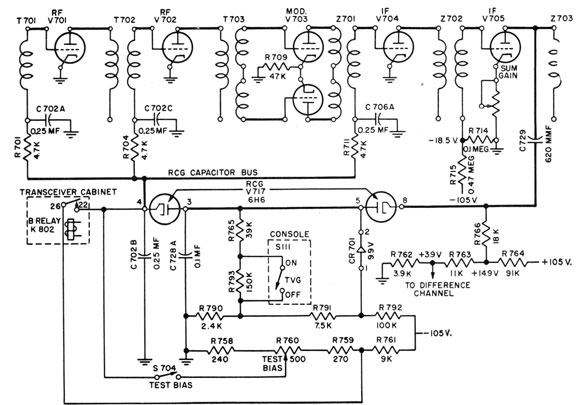
RCG AND TVG CIRCUITS
The RCG and TVG (time varied gain) circuits
are arranged to control the grid bias of the r-f
stages in the receiver channels and thus to reduce
the receiver sensitivity during transmission and
heavy-reverberation periods. A reverberation-controlled gain in the audio channel restores the
output as the reverberation level decreases along
the particular bearing to which the audio system
is trained. The gain recovery of the video channel
is identical with the audio channel and employs
the RCG voltage. The circuits producing this
voltage use V712 and one section of twin triode,
V713.
During the interval preceding a transmission
pulse, the control grid of V713 is maintained at
approximately -80 volts, with respect to ground,
by a divider connected between the keying pulse
line and the o105 volt bias. The cathode is
connected to approximately a -60 volt point
on another dividing network connected to the
same -105 volt source. In this condition the
grid bias is maintained at cut-off. The keying
pulse changes the voltage between grid and ground
raising the grid voltage above cut-off. This rise
in grid bias in a positive direction allows the tube
to conduct, thus charging the RCG bias capacitor, C715, negatively to ground. At the
end of the keying pulse, the grid of the TVG
control tube, V713, is restored to approximately
-80 volts with respect to ground and the tube
no longer conducts.
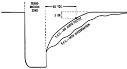
The RCG bias capacitor can then discharge
through the resistors shunted across it and through
half of diode, V712. The time constant is such
that the voltage of the capacitor, if used for grid
bias in the gain-control tubes of the receiver,
restores the gain to within 5 db of its original
value at a time corresponding to a range of 80
yards, provided there is no d-c voltage across the
other half of the diode, as would normally be
produced by an audio output signal. This
voltage and gain recovery is defined as TVG and
is illustrated in figure 7-3.
Figure 7-3 -TVG and RCG bias.
Reverberation control of gain is affected by
retarding this recovery as a function of audio
output level. The primary voltage of the audio
output transformer is coupled to one cathode of
the duodiode, V712, through a capacitor and
current-limiting resistor. Rectification by this
diode produces a d-c voltage across the resistor
R755 of the diode proportional to the audio
level. This voltage is applied to the second
half of V712 through R756 and causes the discharge of C715 to be retarded. The discharge of
the RCG bias capacitor, C715, through the
second diode section of the RCG control tube,
V712, can proceed only when the potential on
C714 is less than that on C715. As the reverberation and thus the d-c voltage across the
capacitor C714 decrease, the RCG bias capacitor
can discharge further, allowing the gain to
increase. An increase in reverberation level
cannot, however, decrease the gain. When the
reverberation level is high and persistent, an
overriding control is provided by the shunting
action of the 2.2-meg resistor across the RCG
bias capacitor. This shunt resistor allows the
capacitor to discharge independently at a slow
rate, whether or not the audio level allows it to
discharge through the diode. This RCG voltage
(figure 7-3) is supplied to the grid circuits of the
r-f stages of the audio and video channels.
The same RCG bias that is supplied to the audio
channel is used in the video channel. Because it is
not desirable for the gain of the video and the gain
of the audio channel to depart from some desired
ratio one to the other. Otherwise, it might cause
an absence of audio or video signals, depending on
which gain is lower. Under normal conditions the
reverberation is sufficiently omnidirectional to produce satisfactory operation.
UNICONTROL OSCILLATOR
The unicontrol oscillator (figure 7-2), tunable
from 87 kc to 94 kc supplies the screens of the first
mixer tubes in the video and audio channels of the
receiver. It also supplies the converter circuit for
producing the frequency to be transmitted. The
unicontrol oscillator, half of V714, is a Hartley
oscillator. The oscillator employs a center-tapped
inductor, tuned by four capacitors and a section of
the main tuning capacitor. A value of inductance
was chosen to provide good tracking with the t-r-f
stages of the receiver. The padding capacitance,
C770 and C795, helps to provide tracking with the
t-r-f circuits. The remaining two capacitors C769
and C768 are a trimmer and fixed capacitor.
The voltage from the center tap of the inductor
of the Hartley oscillator is supplied to the high-impedance grid circuit in the converter by means of
a series resistor and capacitor. This same voltage
is supplied to the control grid of the second triode
section of V714. This section (a cathode-follower)
provides screen grid modulation to the first mixer
tubes, V703 and V708, in the video and audio channels, respectively. Since the screen grid voltage is
supplied from the large unbypassed cathode resistor of the cathode-follower the screen voltage will
be very low during the negative half of the input
signal to the cathode-follower. The result is a
screen voltage that is low for an appreciable part of
each cycle. This mode of operation results in improved mixer action and provides better discrimination against undesired frequencies.
BEAT-FREQUENCY OSCILLATOR
The beat-frequency-oscillator (BFO) circuit,
figure 7-2, consisting of one section of twin triode
V715 and reactance tubes V716 and V717,
153
modulates the screen voltage of the second mixer, V709,
in the audio channel of the receiver in order to produce an audio note from the received signals. The
oscillator frequency is controlled by the target-doppler-nullifier and own-doppler-nullifier control
tubes, in response to the functioning of the doppler-nullifier circuits. The oscillator consists of a Hartley circuit with grid leak bias and cathode degeneration for stability. The oscillator coil assembly is
an arrangement of three inductors and two blocking capacitors, which provide (1) a center tap for
the oscillator cathode and (2) d-c isolation for the
anodes of the reactance tubes. The center tapped
inductor functions in parallel with tuning capacitor
C775 and is effectively in parallel with the plate
circuits of the reactance tubes.
A resistance of 50 ohms, composed of two
resistors, R778 and R781 in parallel, in series
with capacitor C774 is used as a phase-shifting
circuit. The voltage across R778 and R781 leads
the output voltage of the oscillator circuit by
nearly 90° and is the a-c grid signal for the reactance
tubes. Each of these tubes has suppressor resistors in series with its grid to prevent spurious
oscillations. Both tubes are cathode-biased. The
screen voltage comes from the regulated 150-volt
supply. The reactance tube, V716, controls the
BFO in response to the ODN circuits, whereas
tube V717 exerts control from the TDN circuits.
The functioning of the circuit in response to
the d-c controls can be analyzed in the following
manner. Let e represent the a-c voltage developed
across the phase-shifting resistors R778 and R781,
and supplied to the reactance-tube grids. As ip
is in phase with e, the anode current that these
tubes draw from the oscillator circuit leads the
output voltage of the oscillator circuit by 90° and
is thus the equivalent of the current in an adjustable capacitor. The adjustment results from
changes in ip, caused by changes of the d-c grid
voltage. A change of this voltage in the positive
direction increases ip, that is, effectively the
capacitance has increased. This lowers the frequency of the oscillator. Similarly a change of
d-c grid voltage in the negative direction increases
the frequency.
A voltage, taken from the center tap 3, of the
lower inductor supplies the a-c component of screen
voltage through R744 to the second mixer, V709,
in the audio channel.
DOPPLER-NULLIFIER CIRCUITS
The doppler-nullifier circuits, which provide
the d-c control voltages for the BFO, consist of an
audio amplifier and limiter, a power amplifier
stage, V719, a discriminator, and relay control
circuits.
Audio Amplifier and Limiter
The audio frequency voltage, developed at the
anode of half of the first audio amplifier, V710, is
coupled to potentiometer R810 (labeled "D. N.
GAIN") for the purpose of adjusting the amplification of the audio circuit to a value adequate for
doppler nullification. The signal from the potentiometer is coupled to the grid of V718 through a.
low-pass RC filter to reduce any 65-kc signal component present in the audio channel. The series
resistor R811 limits the input grid signal on the
positive half cycle. The increase in plate current
at this time is further limited by the degenerative
action of the unbypassed screen voltage supply.
The cathode bias is such as to limit the plate
current on the negative portion of the input
signal. Thus essentially a square wave output of
approximately constant amplitude is produced
from V718. This is desirable because the input
to a frequency discriminator should vary only in
frequency.
The square-wave output is coupled to the
control grid of beam-power tube V719 capacitively
and through a current-limiting resistor. Because
of the necessity for preserving the square-wave
character in the incoming signal, the power stage
employs negative feedback provided by the
unbypassed screen supply and cathode resistor.
Capacitor C776 and five series resistors are
connected across the primary of the output
transformer to reduce the shunting effect of the
primary inductance by making it part of a low-Q
parallel-resonant circuit in the vicinity of the
800-cps frequency. The result is a voltage from
the secondary of T705, which approximates a
constant amplitude square wave which is coupled
to the discriminator.
To make the doppler-nullifier circuits inoperative when the equipment is in the listen condition,
one-half of twin triode V715 is used to cut off the
beam-power tube, V719. In the listen condition,
the keying selector on the front panel of the
154
sonar-indicator-control unit, connects the keying
pulse line to a circuit of -105 volts with respect
to ground. Conduction occurs in V715 which
effectively connects a voltage divider circuit
comprising V715 and resistors R816 and R817
from the keying pulse line to ground. This action
biases the grid of the beam-power tube to cut-off.
The need for a zero output is explained in connection with the ODN operation in the following
paragraphs. When the equipment is echo ranging,
this keying pulse line is normally at +45 volts
above ground, and it pulses to +220 volts during
transmission. Under these conditions, the diode-connected half of V715 cannot conduct and it has
no effect on the operation of power amplifier V719.
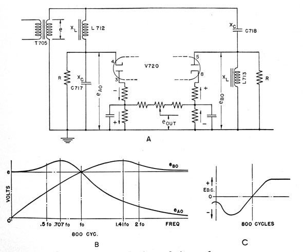
Discriminator Circuit
The function of the discriminator circuit is to
produce a d-c voltage that is proportional to the
deviation of the audio frequency from the reference
of 800 cycles per second. This function is accomplished by a circuit that produces voltages whose
amplitude is proportional to the variation in
frequency and a comparison rectifier with a
filtered output.
The discriminator circuit (figure 7-4) functions
in a manner somewhat similar to the ratio detector
used with f-m circuits at higher radio frequencies.
For the discriminator circuit of figure 7-4, the d-c
voltage produced by rectifier V720 must be
Figure 7-4 -Discriminator. A, Equivalent circuit; B, voltage curve; C, output curve.
155
positive for audio frequencies above 800 cycles
per second and negative for frequencies below
this value; and there must be no secondary
crossover points due to harmonics of frequencies
which are below 800 cycles per second. The input
impedance of the circuit shown in figure 7-4, A,
is constant and equal to R/2 over the range of
frequencies involved. It is therefore a desirable
load.
The voltage across the parallel combination of
resistance and capacitance is shown as curve eAO in
figure 7-4, B, whereas that across the resistance-inductance combination is shown as curve eBO in
the same figure. These two voltages are equal to
each other at a frequency such that the inductive
and capacitive reactances are equal. The ratio
of these two voltages is approximately 4-to-1 at the
frequencies which are either one-half or twice the
center frequency. One of the two desired output
voltages is produced to ground across capacitor
C717 and the other across inductor L713.
These two voltages, eAO and eBO are rectified
by the two sections of twin diode V720. Resistors
are placed in series with the rectifier loads to
produce d-c voltages that are proportional to the
average value of the a-c voltages, rather than to the
peak values, to minimize the effects of waveform
distortion. The a-c voltage across the capacitor
varies inversely with frequency while that across
the inductor varies directly with the frequency.
Thus, the a-c voltage that varies directly with
frequency produces a positive d-c voltage output
from V720, while the a-c voltage that varies
inversely with frequency produces a negative d-c
voltage output. These voltages are developed
across separate RC filter combinations. The difference between these two d-c voltages is developed
across three resistors in series connected across the
two filters mentioned. A close adjustment of the
exact frequency that produces zero d-c voltage is
made possible by the center resistor of the three,
which is a potentiometer, so that this zero-voltage
point can be made to coincide exactly with the
center frequency of the audio peak filter in the
audio channel.
A typical d-c voltage curve from the discriminator circuit is shown in figure 7-4, C. For
frequencies above 800 cycles per second this voltage is positive, and for frequencies below 800
cycles per second it is negative. The value of this
voltage decreases as zero frequency is approached
because the audio response falls off at very low
frequencies. At zero frequency, there is a small
residual voltage that is due to power-supply ripple.
The discriminator output voltage is supplied to
relays K702 and K703 for use in the ODN and
TDN operations.
Own-Doppler-Nullifier Circuit
The combination of the BFO with reactance
tubes and of the audio amplifier with discriminator
circuits provides a means of making the audio
frequency correct itself to the reference frequency
of 800 cycles per second. It is similar to a servo
system in which the audio-frequency input deviation produces a d-c voltage output that helps to
restore the frequency of the input signal to normal.
The total feedback is about 30, which means that
the audio frequency deviation is reduced to one-thirtieth of that which would be obtained without
doppler nullification.
For ship's own doppler nullification (ODN) the
circuits function in the following manner. During
the interval between transmission pulses, the
keying pulse line remains at +45 volts to ground.
The grid, terminal 4, of V713 is held at its cathode
potential (approximately +5 volts to ground) by
grid current and C723 charges to about 40 volts.
During transmission when the keying pulse line
rises to +240 volts for a period of 35 milliseconds,
capacitor C723 in the grid circuit of the second
section of V713 is charged by grid current to
approximately +235 volts. During the period
of this pulse, the ODN sampling relay is not disturbed, but remains closed-its normal position-for its current change is very slight. At the end
of the transmission, when the keying pulse line
is restored to +45 volts, the grid of the tube is
carried to approximately -190 volts with respect
to ground by the charge retained on the grid
capacitor. This action cuts the tube off, and the
sampling relay, K702, drops out. (Capacitor
C726 is shunted across second section of V713 to
reduce the otherwise severe voltage transients.)
The grid capacitor C723 discharges towards +40
volts, and as the grid potential approaches +5
volts with respect to ground a point is reached at
which the tube current is again sufficient to operate
the sampling relay, which remains energized until
156
the end of the next keying pulse. During the
time this relay is de-energized, it applies the output of the discriminator to the ODN reactance
tube, V716, as a d-c grid bias.
During the sampling period, which is equivalent
to approximately 250 yards of range, capacitor
C710 in the grid circuit of reactance tube V716
acquires a charge from the frequency-discriminator
circuit. Resistor R858 placed in series with the
charge path of the capacitor sufficiently lengthens
the time constant to enable the circuit to average
the frequencies present in the reverberation and
to approach a true solution for own ship's doppler.
When the sampling relay closes at the end of its
period, capacitor C710 retains a charge which is
applied to the grid of the reactance tube thus
maintaining the audio note at 800 cycles per second. This frequency can shift only as a result of
changes in the charge on the grid capacitor caused
by leakage.
During the sampling period, contacts 4 and 5
on the ODN sampling relay ground capacitor C709
in the grid of TDN reactance tube V717 through
R867 provided that the doppler-nullifier relay is
energized. This relay will be energized when the
equipment is operating in the audio peak condition and the TDN switch is on. The purpose of
this operation is to remove any residual charge on
capacitor C709 that results from the TDN operation and thus to provide the correct initial reference for establishing the ODN circuit control.
After the sampling period, the doppler-nullifier
relay reconnects the TDN circuit to the reactance
tube so that it may function for the rest of the
time, if so desired.
When the equipment is operated in listen condition, the keying pulse line is connected to -105
volts, so that the second section of V713 remains
cut off continuously, and the ODN sampling relay
remains open. The -105 volts on the keying
pulse line cuts off the input to the discriminator
as mentioned previously through the action of
the diode-connected half of V715 with the result
that the BFO remains stable during the listening
operation.
Target-Doppler-Nullifier Circuit
As a means of improving the signal-to-noise
ratio, this receiver can be operated with an audio
peak filter. The audio peak filter comprises a
parallel resonant circuit shunted across the output
of the second triode section of V710. Because
this filter removes off-frequency signals resulting
from target doppler, it is necessary to accompany
its use with a TDN circuit. This circuit functions
in the same manner as the ODN circuit and uses
the same audio amplifier and discriminator to
restore the audio frequency to 800 cycles per
second for all signals.
When the switch on the sonar indicator-control
is thrown to audio peak, it energizes the doppler-nullifier relay, if the equipment is echo ranging,
but not if it is listening. This relay has two
functions-(1) it grounds one terminal of the audio
peak filter, making it operative, and (2) it connects
the discriminator output to the grid reference capacitor C709 of the TDN reactance tube through
the sampling relay when the latter is energized.
During the reverberation sampling immediately
after transmission, before the sampling relay closes,
the discriminator is connected to the ODN reactance tube in order to set the BFO for an audio
output of 800 cycles per second from the reverberation. At the end of this period, when the
sampling relay recloses, the discriminator output
is applied to the grid circuit of the TDN reactance
tube, and all signals thereafter are restored to the
same reference. The TDN circuit can be disabled
by closing switch 5701, which allows (1) echo
ranging on fixed targets with the audio peak
filter and (2) the use of the ODN circuit alone.
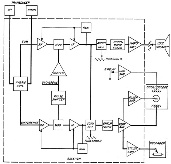
Sum-and-Difference Receiving System
To convert the echo-signal phase-angle difference between the two halves of a split transducer
into a polarized magnitude difference, either a
sum-and-difference or a comparison system must
be used. In operation, there is very little difference between the results of the two systems, and
their complexity is about the same. The receiver
239276°-53-11
described here uses a sum-and-difference system
and is part of the Model QDA depth-determining equipment.
UP-DOWN DEFLECTION
In the discussion of this receiver, when the echo
is returned from a target below the axis of the
157
Figure 7-5. -Block diagram of the QDA receiver.
transducer, a down voltage is developed. This
down voltage indicates that the phase of the signal
from the lower half of the transducer is leading
that of the upper half, and it is necessary for the
operator to train downward to obtain the correct
depression angle.
Similarly, when the echo is returned from a
target above the axis of the transducer, an up
voltage is developed, indicating that the phase of
the signal from the upper half of the transducer is
leading that from the lower half. In this case it
would be necessary for the operator to train upward
for the correct depression angle.
The circuits that produce the up and down
voltages, together with the indicating unit, are
called the depth deviation indicator (DDI).
In azimuth equipments, operation is very similar, except that the plane of operation is rotated
158
Figure 7-6 -Hybrid-coil input circuit.
90°, and down and up become right and left. The
unit is then called the bearing deviation indicator
(BDI).
Figure 7-5 is a block diagram of the QDA
receiver. The voltages from the two halves of
the transducer are combined in a hybrid coil.
This coil has two output voltages, one of them
being the sum of the up and down voltages, the
other being the difference or diff, as it will be
referred to, of the up and down voltages. These
two output voltages are then amplified in separate
receiver channels. The two channels are very
similar, each consisting of two stages of r-f amplification, a modulator, and a 2-stage i-f amplifier.
The two channels are controlled independently by
means of two RCG circuits.
Because of the use of RCG circuits, the reverberation outputs of the sum and diff channels are
substantially constant. Thus a d-c bias may be
introduced in series with the conjugate detector of
the proper magnitude to prevent the reverberation noises from appearing at the output. However, any noise or signal of greater magnitude than
the average reverberation level appears on the
deviation indicator scope as a distinct pulse.
This bias is known as threshold control and is
manually controlled by a potentiometer located
on the receiver chassis. With this control, the
threshold voltage may be set as close to the average
reverberation level as desired, or it may be removed from the circuit entirely.
The output of the conjugate detector is supplied
to the vertical deflection coils of the DDI through
the vertical deflection amplifier, which converts
the positive and negative d-c signals of the detector
into the proper voltage for the operation of the
cathode-ray tube.
The horizontal-sweep generator in the block
diagram of figure 7-5, controls the left-to-right
traverse of the electron beam of the DDI cathode-ray tube. The sweep progresses from left to right
at a nonlinear rate. The nonlinearity of the sweep
is evidenced by the fact that during the first half
of the sweep the beam travels a time equivalent
to 500 yards of sonar range, whereas during the
second half of the sweep the sweep requires twice
that time, or the equivalent of 1,000 yards of range,
to travel the same distance.
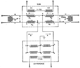
The hybrid coil used in this receiver is shown
in figure 7-6. The signals from the separate halves
of the transducer are connected at the inputs
marked "E." The signal current in the primary
windings 4-5 and 5-6 of the sum transformer is
proportional to the vector sum of the up transducer
voltage, and the down transducer voltage. The
sum may be checked by observing the instantaneous polarity markings at the two sources and the
direction of the arrows in the figure. Thus, the
voltages induced in the two sections of the primary
winding of the sum transformer combine to produce an output which is proportional to the vector
sum of the voltages from the two halves of the
transducer.
If the transducer voltages are equal and in
phase-a condition which would exist when the
Figure 7-7 -Sum and diff voltages related to up and down
phases.
159
target is exactly on the axis of the transducer-the
up and down voltages are in series and in phase so
that the voltage on the low side of the sum transformer is represented by 2E. If the ratio of the
transformer is N for the secondary winding (S1
and S2 in series) to the four primary windings (P1-P4 in series), the secondary voltage for the on-target case will be 2NE.
For the on-target case the potential difference
between points 2 and 5 is zero, because the two
transducer voltages, being of equal magnitude are
opposite in phase and subtractive in their effects
across these points. Under these conditions no
current flows through the diff half of the transformer because this half is connected across points
2 and 5 and the output of the diff channel is zero.
If the voltages from the two halves of the transducer are equal and 180° out of phase, the output
of the sum channel will be zero, and the output of
the diff channel will be 2NE, which is the same as
the output voltage of T701 for the on-target case.
If the target is above the axis of the transducer
the signal coming to the upper half of the transducer arrives before that coming to the lower half,
resulting in a phase differential between the two
signals. The relative magnitudes of the two signals
is approximately the same, because the difference
in range between the upper and lower half of the
projector is a very small percentage of the total
range to the target. If the target is above the axis
of the transducer, the signal supplied to the up
input of the hybrid transformer leads that supplied
to the down input, and results in a potential
difference between points 2 and 5 of figure 7-6.
Thus, at that instant, 5 is negative and 2 is positive, the direction of instantaneous current flow is
indicated by arrow A, for the polarities shown, and
results in an output from the diff channel, which is
proportional to the phase difference between the
up and down signals.
If the target is below the axis of the sound beam,
the signal supplied to the down input is leading the
signal supplied to the up input. This results in a
180° phase shift from the preceding case. Thus,
at the instant that point 2 is negative, point 5 is
positive and the current flows in the direction
indicated by arrow B. Note the direction is
opposite to that existing when the up input was
leading. Thus the difference signal when the up
Figure 7-8 -Vector diagrams of input voltages.
160
signal is leading, is displaced 180° with respect to
its phase when the down signal is leading. Figure
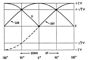
7-7 shows a plot of the amplitude of the sum and
diff voltages as a function of the phase angle
between the up and down voltages.
Figure 7-8 shows that when the target is above
the transducer axis the sum voltage lags the diff
voltage by 90° and when the target is below the
axis the sum voltage leads the diff voltage by 90°.
It is not possible algebraically to add two voltages
in quadrature. In order to overcome this difficulty
the diff voltage is shifted 90°. The solid curves of
figure 7-7 show the relative magnitudes of the sum
and diff voltages. These curves are not coincident
in time. The dotted curve with the solid curve
labeled "diff" in the figure shows the diff voltage
after the phase has been shifted 90°. This shifted
voltage can now be added directly to the sum
voltage in the conjugate detector.
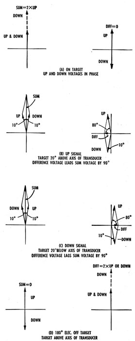
Consider the instantaneous signal at the up and
down hydrophones of some particular amplitude,
E. For an on-target signal, the two voltages are
in phase. The diff voltage is zero and the sum
voltage is 2E. If the echo originates above the axis
of the transducer, up leads down, but if the echo
originates below the axis of the transducer, down
will lead up.
Figure 7-8, A, shows a vector diagram for an
on-target signal. Suppose the up voltage leads
the down voltage by an angle θ. Figure 7-8, B,
illustrates this case for θ equal to 20 electrical
degrees, or about 0.4 mechanical degree. Because
the vectors are equal in magnitude, it follows from
the geometrical construction of sum and diff, that
for any up signal the diff leads the sum by 90°.
Similarly, figure 7-8, C, illustrates that if the up
voltage lags the down voltage by an angle θ, the
diff voltage lags the sum voltage by an angle of 90°.
In figure 7-8, B and C, it is shown that the phase
of the diff voltage with respect to the sum voltage
changes by. 180° as the returned echo changes
from up to down. The conjugate detector uses
this fact to determine whether the trace of the
DDI scope is deflected up or down.
Figure 7-8, D, illustrates the difference of 180
electrical degrees between the up and down voltages produced by a target that is approximately
4 mechanical degrees above the axis of the transducer. This case is similar to the on-target case
except that now the sum is zero and the diff is
equal to twice either the up or the down voltage.
From the foregoing discussions and the geometry of figure 7-8 it can then be concluded that:
1. The amplitude of the sum voltage is equal to
2E cos θ/2, where θ is the electrical phase difference between up and down.
Figure 7-9 -R-f amplifier.
161
Figure 7-10 -Typical frequency characteristics, input circuit,
and r-f amplifier.
2. The amplitude of the diff voltage is equal to
2E sin θ/2.
3. The sum and diff voltages are always 90°
apart.
4. As the diff voltage goes through zero amplitude, at zero phase difference between up
and down, the phase of the diff voltage
changes by 180°.
5. If the up voltage leads the down voltage,
the diff voltage leads the sum voltage by 90°.
6. If the up voltage lags the down voltage, the
diff voltage lags the sum voltage by 90°.
R-F AMPLIFIER
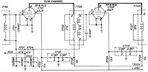
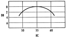
The r-f amplifier is shown in figure 7-9. It is a
typical 2-stage transformer-coupled amplifier.
The input transformer has sufficient voltage gain
to reduce the effects of inherent tube noise. The
secondaries of the coupling transformers form
band-pass circuits resonated at approximately 55
kc. The capacitance includes that which is inherent in the secondaries, plus 10 μμf of shunt
capacitance in parallel with the input capacitance
of the tube and circuit wiring. Resistors are
shunted across the primaries of T702 and T703 to
prevent excessive gain and broaden the resonance
curves of the amplifiers.
Grid bias is obtained from the RCG circuits,
which will be discussed later in the text.
A typical gain-versus-frequency characteristic
curve of the input circuit and r-f amplifier is shown
in figure 7-10.
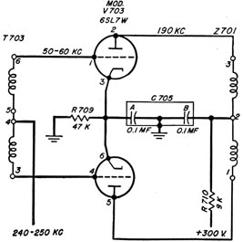
MODULATOR AND PHASE-SHIFT CIRCUIT
It was previously explained that a phase difference of 90° exists between the sum and diff
voltages. For proper operation of the conjugate
detector, which will be explained later, a differential of zero or 180° must exist between these
voltages for the algebraic combination of them.
It follows, then, that the phase of either the sum
or diff channel must be advanced or retarded by
90° to fulfill the zero or 180° relationship.
A phase-shifting network could be placed
directly in the sum or diff channels and effect the
necessary change in phase. However, unless they
are very complex, most phase-shifting networks
are sensitive to changes in frequency. The incoming signal is composed of the transmitter
frequency, the necessary sidebands to produce the
pulse modulation of the carrier, and the 800-cps
modulation frequency, which is used to produce
an audible signal in the audio circuits after detection. A phase shifter which would encompass
this wide range of frequencies would be impractical
because of its complexity. If the network could
be allowed to shift the phase of a single frequency
a much simpler circuit could be devised.
Like all superheterodyne receivers, this receiver
uses an r-f signal from a local oscillator for frequency conversion. In this case the signal is
from the unicontrol oscillator, and the frequency
is from 240-250 kc. This signal, of course, consists of a single frequency.
A review of the theory of modulation will show
that if the frequency of one of the modulation
Figure 7-11 -Modulator.
162
Figure 7-12. -I-F amplifier.
signals is changed in phase, the resultant frequencies will be changed in phase by that same
amount. The derivation of this principle is
complex and is not discussed here.
From the block diagram (figure 7-5) it can be
seen that there is a phase shifter in the circuit
supplying the unicontrol oscillator signal to the
diff channel. This network, in effect, retards the
diff signal by 90°, without affecting the sum signal,
which will provide the necessary 180° between the
sum and diff channels.
Then, the sum and diff are in phase for any up
signal, and the amplitude of sum+diff is simply
the sum of the amplitudes. For any down signal
the two voltages are 180° out of phase, and sum+diff is the difference between the amplitudes of
the voltages. Figure 7-7 shows the relation of
the sum and diff voltages to the phase difference
of the up and down signals, after the 180° phase
shift. Curve D, plus the right half of the solid
diff curve, represents the diff voltage after the
phase shifter effect has been introduced.
The modulator circuit is shown in figure 7-11.
The function of the modulator is to convert the
input frequency-which is between 50 and 60 kc-to a fixed frequency of 190 kc by modulating the
input with a variable frequency of from 240 to
250 kc. The 240-to-250 kc oscillator is always
related to the 50-to-60 kc input frequency by a
fixed difference of about 190 kc. This difference
is maintained in the oscillator unit by the unicontrol system.
The modulator is a push-pull circuit for the
input frequency of from 50 to 60 kc-that is, the
signals on the grids are 180° out of phase. The
240-250 kc signal introduced between the center
tap of the input transformer and ground makes
the 240-250 kc signals on the two grids in phase
and this frequency is suppressed in the output.
The sum and diff frequencies are obtained most
effectively by biasing the two tubes nearly to
cut-off on no signal.
The principal output frequencies are the input
frequency (50 to 60 kc), the sum frequency (290 to
310 kc), and the difference frequency (190 kc).
The input and sum frequencies, as well as products
of higher order, are suppressed in the output by the
plate load impedance, which acts as a band-pass
filter that passes frequencies in the 188.4-to-191.6
kc band.
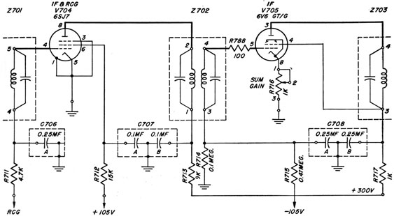
I-F AMPLIFIERS
A schematic of the i-f amplifiers is shown in
figure 7-12. There are two of these amplifiers and
163
they are identical-one is used in the sum channel
and the other in the diff channel. The coupling
transformers are of conventional type, having both
the primary and secondary tuned.
The first stage is supplied with RCG bias, but
the second stage is not. The second stage derives
its bias from two sources-(1) from a voltage divider between -105 volts and ground supplying
-18.5 volts to the grid of the stage and (2) from a
variable resistor inserted in the cathode return.
This resistor is marked "sum gain" in the sum
channel and "diff gain" in the diff channel. The
purpose is to provide a means of compensation for
differences in gain between the sum and diff channels. The range of control of each channel is
about 12 db.
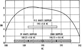
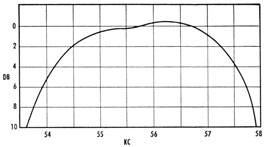
Figure 7-13 -Frequency characteristics of the i-f amplifier.
I-F Bandwidth-Doppler
The bandwidth should be just wide enough to
pass the frequencies necessary for proper performance of the system. If the band were wider the
signal-to-noise ratio would be lowered, with a
consequent loss of weak signals.
The transmitter frequency is 55 kc and is amplitude modulated with an 800-cps signal. The
three principal frequencies transmitted into the
water are 54.2, 55.0, and 55.8 kc. Therefore the
i-f circuit must pass 189.2, 180.0, and 190.8 kc.
The i-f channel frequency characteristics are
shown in figure 7-13.
The effect of the Doppler shift, if the attacking
ship is approaching the target, is to raise the
frequency received. The intermediate frequency,
however, is lowered by this Doppler because the
incoming frequency with its Doppler shift is subtracted from the oscillator frequency to give the
intermediate frequency.
Figure 7-14 -Frequency characteristics of the r-f and i-f
amplifier combination.
Figure 7-13 shows that the zero doppler condition is displaced to a center frequency of 190.75 kc,
thus allowing the shift caused by a closing range
rate of 39 knots to be passed with only a slight
loss, and a 19.5-knot doppler to pass at full gain.
If the doppler is higher than 39 knots, part of the
lower side band is lost, and at 58 knots the lower
side band is lost completely, resulting in a 2.5-db
loss in signal-to-noise ratio. In the opening doppler condition, the upper side band is lost at 19
Figure 7-15 -Phase-shifter and buffer circuits.
164
Figure 7-16 -Conjugate detector and envelope filter.
knots. Even with the 2.5-db loss, the signals are
usually strong enough to permit satisfactory operation at 58 knots closing and 19 knots opening.
The over-all characteristics of both the r-f and i-f
stages are shown in figure 7-14.
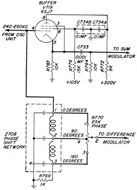
PHASE-SHIFTER AND BUFFER CIRCUITS
It has been explained that the 240-to-250 kc
signal from the oscillator is supplied to the sum
circuit through a buffer and to the diff circuit
through a phase shifter, in order to obtain the
proper zero or 180° phase relation between the
sum and diff signals.
The phase difference between the two channels
(shown in figure 7-15) is obtained by shifting the
phase of the 240-250 kc supply to the diff channel
with respect to the supply to the sum channel. In
order to compensate for phase variations between
the two channels inherent in manufacture, a
phase-shift compensation has been incorporated
in the phasing circuit. The phase-shift network
has three fixed taps corresponding to 0°, 90°, and
180°. The 0° and 180° points are connected to
opposite ends of a potentiometer and the 90°
point is connected to the center of the potentiometer. The output of the circuit is taken from
the moving arm of the potentiometer. As the
phasing potentiometer is rotated through its
range, the phase of the input to the diff modulator
shifts smoothly and continuously from 0° to 180°
with respect to the 240-250 kc signal from the
oscillator with about a 3-db change in amplitude.
The network in conjunction with the phase
potentiometer, inserts an average phase shift of
90° with ±90° available for compensating purposes.
The 240-to-250 kc supply is connected to the
sum modulator through a cathode-follower buffer
stage with essentially no gain or loss and zero
phase shift. The purpose of the stage is to prevent crosstalk between the strong signal in the
sum channel and the weak signal in the diff channel for the on-target condition.
165
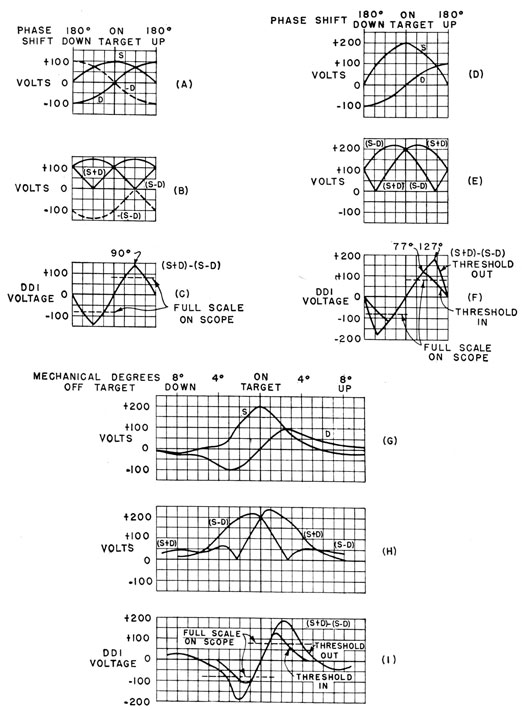
Figure 7-17 -Derivation of DDI voltage from sum and diff.
166
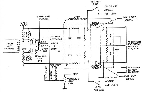
CONJUGATE DETECTOR
The primary purpose of the conjugate detector
is to combine the sum and diff voltages so that an
up voltage produces an up deflection on the
cathode-ray tube, a down voltage produces a down
deflection, and an on-target signal produces no
deflection at all or equal deflections in both directions. Figure 7-16 illustrates the schematic circuit of the conjugate detector and envelope filter.
The circuit is arranged so that the (S+D) (sum
+diff) voltage is peak-rectified in the upper
section of V714 and the (S-D) voltage is peak-rectified in the lower section. The terminology
"S+D" and "S-D" is arbitrary, and is used to
indicate that the sum and diff signals add in one
circuit and subtract in the other.
The following equations apply to an assumed
transducer:
Esum-=NE cos θ/2
Ediff-=NE cos θ/2
The practical transducer used with this system
differs somewhat from the theoretical transducer
assumed in the sine and cosine relation. However,
the performance is developed for the case assumed
and then is compared with the practical case.
The sine and cosine relation is shown graphically
in figure 7-17, A, in which the peak amplitudes
of the sum (S) and diff (D) curves are assumed to
be equal, the equality being established by the
RCG circuit, which will be discussed later. Also
plotted is -D, which is used in determining
(S-D).
Figure 7-17, B, shows a plot of (S+D) and
(S-D) as the electrical phase between up and
down is varied. This plot can be thought of as
either (1) the peak a-c voltage applied to the
rectifier (figure 7-16) without regard to phase,
or (2) the d-c voltage after rectification. The
-(S-D) curve is also shown, as it is used in
determining the output of the conjugate detector.
The (S+D) and (S-D) curves indicate what is
actually measured with respect to ground on
the leads marked "sum+diff" and "sum-diff"
in figure 7-16.
However, the difference between these two
voltages is used to deflect the spot on the cathode-ray tube. In order to produce the currents necessary for deflection, the voltage output of the
conjugate detector is supplied to the vertical
deflection coils of the magnetically deflected
cathode-ray tube through vertical deflection amplifiers. If an on-target echo is received, the
(S+D) and (S-D) voltages are equal, and two
pulses of equal amplitude are sent to the deflection coils. The windings of the deflection coils
are wound in such a manner that these currents
oppose each other and the net flux produced is
zero, so that the spot is not deflected. If an up
signal is received the (S+D) voltage is always
greater than the (S-D) voltage and the currents
establish a field that deflects the spot in a manner
that indicates to the operator the deviation from
true depression angle. For a down signal the converse applies.
A plot of this function, as the up-down phase
shift is varied, is shown in figure 7-17, C. because d-c potentials are used, a plus sign indicates
a positive potential for an up deflection on the
cathode-ray tube, and a minus sign indicates a
negative potential for a down deflection on the
cathode-ray tube. This plot is known as the
DDI window, because it shows the window width
through which the system is sensitive.
Zero potential is obtained for zero phase shift,
which corresponds to an on-target signal. Zeros
are obtained also for +180° and -180°, which
are not on target but are approximately 4 mechanical degrees off-target. For the practical transducer, however, the probability of ambiguity is
very small, as the amplitude of the echo at 4° or
more off-target is approximately 15 or 20 db
below the amplitude for on-target. It can be
seen that the peak amplitude of the BDI deflection occurs at ±2 mechanical degrees.
For simplicity, the sum and diff voltages in the
receivers, figure 7-17, A, are shown as being equal.
In actual practice, however, the sum voltage is
made approximately twice the diff voltage in
order to improve performance. This relation is
accomplished by constructing the output coupling
transformer of the sum channel to have a voltage
gain of 6 db higher than that of the diff channel.
The curves for these operating conditions are
shown in figure 7-17, D, E, and F. From a
comparison of figure 7-17, C, and figure 7-17, F,
the effects of increasing the sum voltage can be
seen. The peak amplitude shown in figure 7-17,
F, is at approximately 127 electrical degrees,
rather than at 90°.
167
Figure 7-18 -Effects of the threshold circuit.
168
Figure 7-19 -Simplified schematic of the RCG circuit.
The preceding discussion was on the basis of
an ideal transducer. A practical transducer has
a somewhat different performance. This performance is shown in figure 7-17, G, H, and I,
plotted in mechanical rather than electrical degrees,
The effects of the threshold-out and threshold-in
curves will be explained later. Beyond ±5
mechanical degrees a reversal is obtained so that
up indicates down, and vice versa. However, the
sensitivity of the transducer beyond 5° from the
axis, is so low that unless the echo-ranging conditions are exceptionally good the signals are lost
in the ambient noise and reverberation.
DDI THRESHOLD CIRCUIT
In figure 7-16 a potentiometer is shown connected between the -105 volt supply and ground,
with the moving contact supplying this variable
voltage to the plates of the conjugate detector.
This potentiometer is called the threshold control,
and its purpose is to produce an apparently higher
signal-to-noise ratio in the DDI. It accomplishes
this function by placing a bias on the plates of the
conjugate detector, variable in magnitude from 0
to approximately -105 volts. The control is
preset at the factory to provide a bias of -85
volts. This bias is of such a value that most of
the noise is not rectified, but the signal plus noise
rides above the threshold voltage. The variable
supply to the diode is bypassed to ground by a capacitor, to provide a low a-c impedance to ground,
regardless of the setting of the potentiometer.
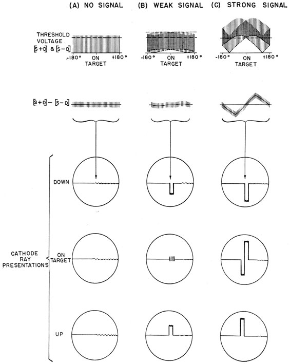
Previously, when the conjugate detector was
discussed, the effect of noise was not considered.
Figure 7-18 shows the (S+D) and (S-D) voltages, (S+D)-(S-D) , and the presentation on the
cathode-ray tube. Figure 7-18, A, shows this
combination for no signal present.
If no signal is present the noise and reverberation, for a particular instant of time during the
receiving interval, are constant and substantially
169
Figure 7-20. -Gain plot.
independent of the tilt of the transducer. This
condition is shown on the (S+D) and (S-D) row
of figure 7-18. The setting of the threshold
potentiometer is at the proper level to allow the
noise and reverberation to just break through the
threshold voltage. Inasmuch as an echo is not
being considered-but noise or reverberation,
which has a random phase relationship among its
many components-the (S+D)-(S-D) plot also
has a random nature. Because of the action of
the threshold bins, the chart shows only the
combination of those parts of the (S+D) and (S-D)
voltages which are greater than the threshold
voltage.
For a weak signal from a target that is exactly
on the axis of the transducer, it is possible that
the resultant of (S+D) and -(S-D) might not
exceed the threshold voltage, with the result that
no indication will appear on the cathode-ray tube.
This condition is not so serious as might be
imagined, however, because most targets are not
exactly at 0°, and if the indication is slightly off-target, the signal overrides the threshold voltage.
In figure 7-17, F, and I, it can be seen that the
DDI voltage plot is altered when the threshold
voltage is applied to the circuit. In the DDI
voltage for the practical transducer (figure 7-17,
I), the effect is to move the point of maximum
voltage from about 2 degrees off-target to 1.3
degrees. It should be noted also in the threshold-out curves that there are secondary patterns
existing beyond ± 5°. If the noise and reverberation conditions are good, these secondary patterns
may give deflections in the wrong direction-that
is, if an echo is 6° below the axis of the transducer,
the cathode-ray tube indicates up rather than
down. If the threshold control is all in, then from
figure 7-17, H, it is apparent that the secondary
pattern is not utilized.
ENVELOPE FILTER
Following the conjugate detector is the envelope
filter network (figure 7-16). The purpose of this
Figure 7-21. -Audio circuit.
170
Figure 7-22 -Typical audio characteristics.
network is to pass the desired frequencies and to
attenuate the undesired noise frequencies. In
this case, the desired frequencies should be spoken
of in terms of pulse length rather than frequency.
The length of the pulse appearing at the output
of the detector is determined by the length of the
transmitter pulse, which, in this system, is between
5 and 50 milliseconds. If the proper R and C
values are selected for the filter, pulses of shorter
than 5 milliseconds length are attenuated. The
800-cps modulation of the output wave, which is
necessary for audio reception, is not used for the
cathode-ray presentation. In fact, the envelope
filter has sufficient loss at 800 cycles per second,
so that this frequency appears only as a fringe on
top of the pulse-if it is not lost in the ambient
noise.
RCG CIRCUIT
The gains of both channels of the receiver unit
are controlled by the RCG circuit, which operates
from the peak amplitudes of the reverberations.
For an echo-ranging receiver the maximum usable
gain is desired at all times so that the weak signals-which are lost if the gain is too small-are
amplified as much as possible for use in the loudspeaker or in the cathode-ray tube. However,
if the gain is too great the ambient noise or reverberation overloads the receiver at some stage so
that signals, normally stronger than the reverberation, also overload and are not recognized. By
means of the RCG circuit, the receiver gain is
adjusted automatically so that the reverberation
is kept at substantially a constant level at the
plate circuit of V705 and at approximately 18 db
below overload.
The RCG action is similar to the AVC action
except that the RCG action is not reversible-that is, the circuit is arranged so that the gain can
increase from a very low initial condition during
the receiving interval but cannot decrease because
the low-gain condition is re-established during each
transmitting interval.
Figure 7-19 shows a simplified schematic diagram of the RCG circuit. During the transmitting interval a potential of about -10 volts is
applied to the grids of the control tubes of the i-f
amplifiers. This potential reduces the transmission through the system by more than 120 db.
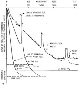
Figure 7-20 shows how the receiver unit varies
in sensitivity because of the time variation of reverberation. Inasmuch as the RCG circuit always produces a constant output of reverberation,
figure 7-20 also shows how the amplitude of reverberation varies with time. This plot can be
shown only in a general manner, because the
amplitude of reverberation is extremely variable.
The actual operation of the circuit is much the
same as that in the dual-channel receiver described
at the beginning of this chapter. One difference
is that in the sum and diff receiver, the reverberation level in the diff channel is approximately 5 db
less than that in the sum channel. Because the
gains of the two channels must be equal or integrally related at all times, it is necessary that two
separate RCG circuits be employed. The only
circuit difference in the two channels is the positive
bias supplied to the RCG detector. The sum
channel detector is biased to approximately +15
volts while the diff channel detector is biased to
approximately +4 volts. This results in a greater
171
RCG voltage supplied to the sum channel and
preserves the relative amplitudes of the signals as
they pass through the sum and diff channels.
This circuit also incorporates a TVG switch.
Its effect when in the on position is to delay recovery of the receiver to about 440 yards. normally with the switch off the gain is restored to
within 3 db of maximum in 100 yards.
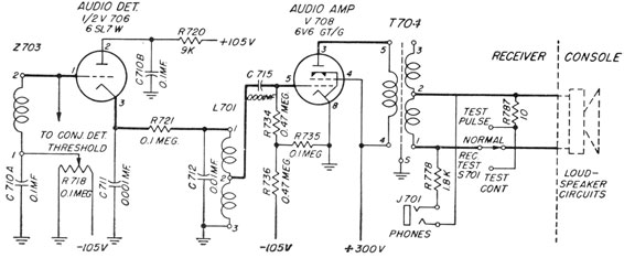
AUDIO CIRCUIT
The audio detector receives its excitation from
the sum input to the conjugate detector. The
schematic of the audio circuit is shown in figure
7-21. The detector operates in a conventional
manner, and the output from it consists of the 800-cps modulation applied to the transmitter and the
noise voltages received by the transducer. The
filter at the output of the detector is sharply tuned
to 800 cycles per second, giving considerable
attenuation to the noise frequencies. Figure
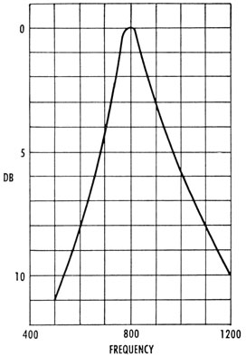
7-22 shows a graph of the typical audio characteristics of the receiver.
A 1-stage audio amplifier of conventional design
is used to amplify the signal to the necessary power
level of about 2 watts.
For test purposes, provisions are made to deliver the output of the audio amplifier to a 10-ohm resistor instead of to the loudspeaker. A
headset jack also is provided with a resistor in
series with it to drop the power being supplied to
the headset to a reasonable value.